Types of Transistors: Here is Quick Overview of BJT Modes
Table of Contents
Why do we call BJT a Bipolar Transistor?
These types of transistors have two PN junctions. BJT has two regions from where conductivity is possible. P-type semiconductor which has the majority of Holes and N-type which has electrons in excess amount form a junction from where conduction is possible due to the movement of charge carriers. When we connect these junctions, we get two regions of conduction, therefore we call it a bipolar junction transistor or BJT in short form.
Construction of Bipolar junction Types of Transistors
A bipolar junction transistor or BJT consists of three terminals; collector, emitter, and base. In this steady-state, device, the current flows through the collector and emitter terminal and we control this current through the base terminal.
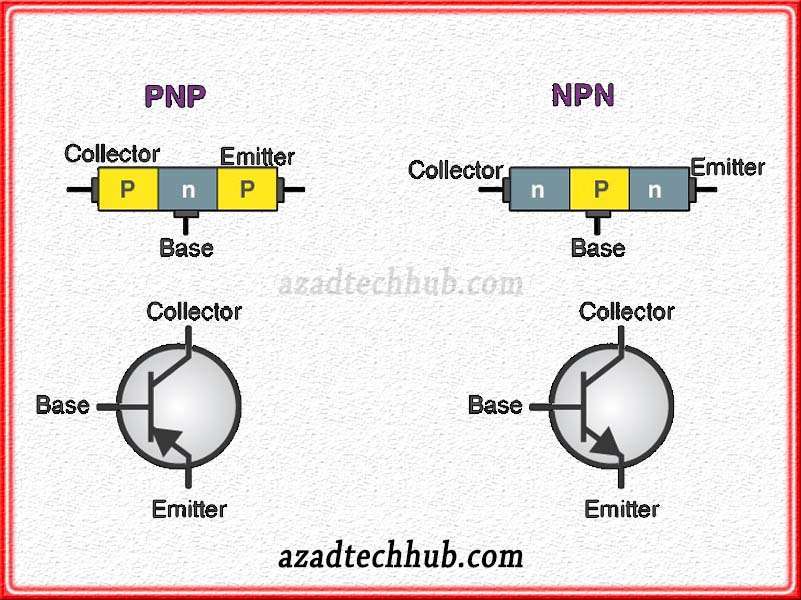
Overall, when we look at the construction of BJT, we see two PN junction diodes together. These PN junctions consist of extrinsic semiconductor material having enhanced electrical properties due to doping of some impurity. There are two main types of BJT including NPN and PNP transistors depending upon the sequence of PN junctions. You can also read about configurations of BJT here. Let’s have a look at the below representation of two types of transistors NPN and PNP bipolar junction transistors.

As per the above discussion, we know that BJT types of transistors have three terminals and now let’s explore more details regarding these terminals.
Emitter
An emitter in BJT is a portion that sends holes or electrons in other portions depending upon the configuration of the transistor. The doping in this region is highest as compared to the other two regions. The base regarding the emitter region is always reverse bias so that the majority of carriers from the emitter region should easily move.
The emitter region or emitter-base junction is always forward bias either as we see in NPN BJT or PNP BJT types of transistors. But there is the main difference between supplying electrons and holes in the case of both transistors. In NPN, the emitter emits the negative charge carriers or electrons to the emitter-base junction. On the other hand, the emitter emits or supplies the positive charge carriers or holes in the case of a PNP transistor.
Base
The doping in the base region is very light and it is a thin region as compared to both the emitter and collector. Whichever charge carriers it receives from the emitter, pass through the collector. This region controls the emitter to collector charge carriers flow and it is a very this region. As it is in between the collector and emitter, so it makes two PN junctions. One with the emitter and the other with the collector terminal. When we look at the doping level, we can say in both types of transistors doping level is the same in the base region.
Collector
This is the third terminal of BJT which receives or collects all the charge carriers emitted by the emitter. The doping in the collector is at a moderate level and doping is less than the emitter region but greater than the base region. The junction between the collector and base is always reverse-bias because it always receives charge carriers emitted by the emitter region. In the case of NPN BJT, it receives the electrons but in the case of PNP BJT, it receives the holes.
Working of Bipolar Junction Types of Transistors
On the basis of positive and negative regions and the doping applied to terminals, we can classify BJT into two types of transistors NPN and PNP; as described above. Both NPN and PNP have two semiconductor junctions. In NPN semiconductors, the “P” doped thin region refers to the anode. While in the PNP semiconductor, the “N” doped thin region refers cathode.
So, the flow of current from the bipolar junction transistor switch occurs when the collector-base region is reverse-bias and the emitter-base region is forward bias. We can operate BJT in three different regions which include active, saturation, and cut-off region.
Active Region of BJT
The collector-base junction is in reverse-biased condition and the emitter-base junction is forward-biased in this mode of operation of BJT. In this way, the current through the collector region “Ic” is controlled or restricted by the current flowing through base “Ib”. The collector and base current are related through the below equation. Where “β” is the gain of the bipolar junction transistor.

As we can see in the above equation, “β” controls the collector current. We see the transistors working in this region mostly in amplifier circuits. Where there is a requirement of high or variable gain. We also call this region a “linear region” because it is in between the saturation and cut-off regions. Normally transistors operate in this region in most circuits.
Cut-off Region of BJT
In this mode of BJT, both junctions of the transistor are reverse bias. We can call this region as “off state” of the bipolar junction transistor. As the transistor behaves like an off switch therefore the collector current “Ic” turns to zero in this region.

To achieve this region, we need to reduce the voltages across the base to such a value that the collector current is zero. Transistor operates in this region when the base-emitter voltages are lesser than 0.7.

As we reduce the voltages lower than 0.7, we see transistor as a switch behaves. Which can actually turn on and off any electronic circuit with high accuracy. we transistor as a switch in many electronic applications like to turn on and off an LED, motor speed control and in many integrated circuits. Gallium Nitride is the semiconductor material which finds applications in Gallium Nitride Charger, Solar Panels and in many integrated basic blocks.
Saturation Region of BJT
Both junctions in this region are forward-biased and the bipolar transistor is in the “ON” state. When we increase the collector current to such a value that after that limit the collector doesn’t increase any further. Hence the saturation condition is achieved and the highest collector current in this state is the saturation current “Isat”.

As the saturation region is achieved, we can say that the transistor is in a short circuit condition. Read about the FET Field effect Transistor, junction field effect transistor or JFET, metal oxide semiconductor field effect or MOSFET.
Read about operational amplifier circuits here.
Follow us on LinkedIn”Electrical Insights” to get the latest updates in Electrical Engineering. You can also Follow us LinkedIn to see our latest posts.

