Types of Field Effect Transistor: A Very Quick Overview
Table of Contents
What is FET? or Field Effect Transistor?
Before diving into the detail of types of field effect transistor let’s just define the field effect transistor. This is a semiconductor device that controls the flow of charge carriers or current with the help of an electric field. Field effect transistors are unipolar in nature and we can also categorize them as single-carrier devices.
The conduction or flow of current through field effect transistors occurs either with electrons or holes. Whereas in BJT (Bipolar junction Transistors), both charge carriers participate in the current flow.
There are several types of field effect transistors (FETs), each with its unique structure and operating characteristics. The main types of FETs include:
Metal-Oxide-Semiconductor Field Effect Transistor (MOSFET): MOSFETs are the most common and widely used types of field effect transistor. They have a metal gate insulated from the semiconductor channel by a thin layer of oxide (usually silicon dioxide). MOSFETs are further classified into two subtypes:
Enhancement Mode MOSFET (E-MOSFET): Requires a positive gate voltage to create a conducting channel between the source and drain terminals.
Depletion Mode MOSFET (D-MOSFET): Has a conducting channel by default and requires a negative gate voltage to “deplete” or reduce the channel conductance.
Junction Field Effect Transistor (JFET): JFETs have a junction between the semiconductor channel and the gate terminal. They are available in two types of field effect transistors:
N-Channel JFET: The channel is composed of n-type semiconductor material, and the gate terminal is p-type.
P-Channel JFET: The channel is composed of p-type semiconductor material, and the gate terminal is n-type.
Insulated Gate Bipolar Transistor (IGBT): IGBTs combine the features of MOSFETs and bipolar junction transistors (BJTs). They are considered to be the important types of field effect transistors. They have a MOSFET input and a BJT-like output, allowing them to handle high voltage and high current levels. IGBTs are commonly used in power electronics applications.
High-Electron-Mobility Transistor (HEMT): HEMTs, also known as HFETs (heterostructure types of field effect transistor) or MOSFETs (modulation-doped field effect transistors), are designed to provide high electron mobility. They are typically made using compound semiconductor materials and find applications in high-frequency and microwave circuits.
Fin Field Effect Transistor (FinFET): FinFETs are a type of 3D transistor structure that overcomes certain limitations of traditional planar MOSFETs. They have a fin-like channel, enabling better control of the current flow. FinFETs are commonly used in advanced integrated circuits (ICs) to achieve higher performance and energy efficiency.
These are some of the main types of field effect transistors. Each type has its advantages and applications, catering to specific requirements in various electronic circuits and systems.
Working of a FET (Field Effect Transistor)
Every FET has a substantial input terminal Impedance. This type of transistor we normally seen in the amplification of weak signals. We can take the example of signal amplification in wireless. The semiconductor path through which current flows, we call a channel.
There are two electrodes on both ends, we call these electrodes the source and drain. In the middle there is a control terminal, we call it a gate terminal. The conductivity of the field effect transistor largely depends on the signal we apply on the control terminal or gate.
The voltage applied to the gate terminal creates an electric field. With the help of this electric field, the conduction area widens inside the channel. This is how a field effect transistor conducts electric current. Let’s have a look at the symbolic representation of a FET Field Effect Transistor.
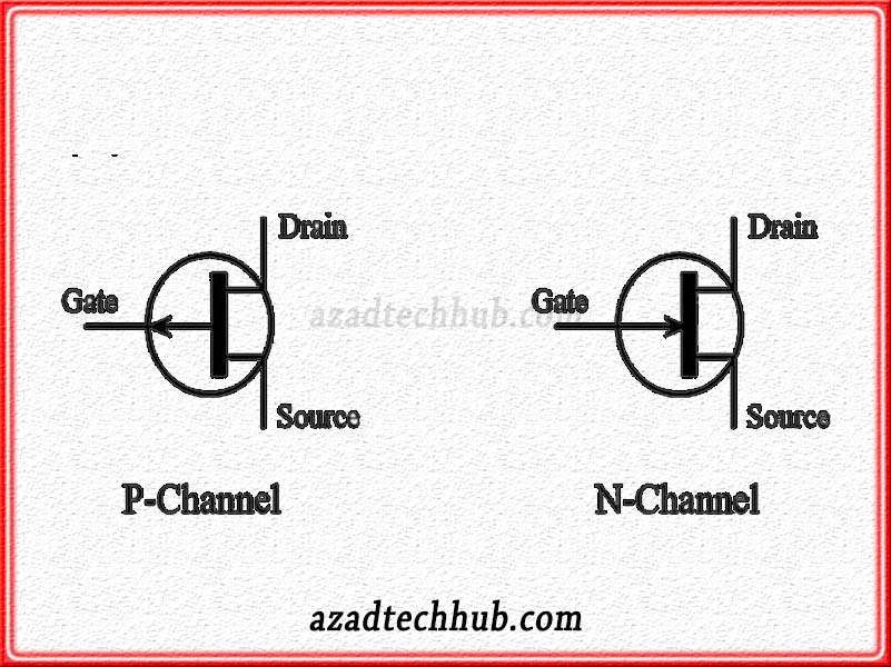
Classification of types of field effect transistor (FET)
We can write down the types of Field effect transistor or FETs into two main categories.
- Junction Types of field effect transistor or in short form as JFET
- Metal Oxide Semiconductor types of field effect transistor or in short form as MOSFET
We can classify both transistors as p-channel or N-channel depending upon their construction. Whereas the MOSFET is further divided into enhancement and depletion types.
Construction of Junction Types of field effect Transistor (JFET)
This transistor has three terminals. Where two terminals are at both ends just like a simple FET. The third terminal is in between the other two terminals which control the conduction of current between them. JFET or Junction field effect transistors as explained above are two types p-channel and n-channel type. We can have a look at the below construction of p-channel and n-channel JFET.
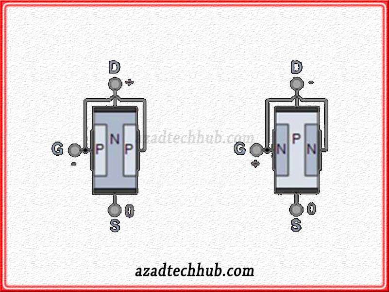
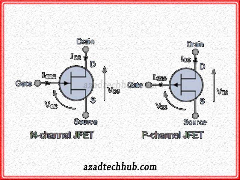
Circuits Representations of N-Channel & P-Channel JFET
In both types of JFET, voltages across the source and the gate terminal are denoted by “VGS”. The drain and source potential is represented by “VDS”.
In an n-channel Junction field effect transistor, there is a small terminal of an n-type semiconductor material but larger p-type semiconductor materials are diffused on opposite ends making two PN junctions. The two P-type semiconductors diffused at both ends are connected somehow externally or internally and we call it the gate terminal.
On one end we can call the source terminal. The other terminal we can call the drain of the Junction field effect transistor. From the source, the majority of charge carriers (electrons in the n-channel case) enter the JFET and they leave through the drain. In the middle of the gate terminal, we can control the number of carriers entering from the source and leaving through the drain.
The silicon bar in between source “S” and drain “D” just works like a resistance. We can resemble the gate terminal of a JFET with the base terminal of a bipolar junction transistor or BJT. Also, we can say that the source and drain terminals are similar to the emitter and collector of bipolar junction transistor “BJT”. Read More about BJT Modes and BJT configurations.
Working of Junction Field Effect Transistor(JFET)
In normal conditions, the two p-type regions for two PN junctions with the n-type semiconductor channel. The depletion regions of these PN junctions in this scenario are of equal width and uniform. When we apply the voltages between the drain and source “Vds” and keep the voltages between the gate and source zero (Vgs=0), A very high current passes through the channel.
This happens due to the depletion region. Which becomes very thin after applying the voltages between the drain and the source. Let’s have a look at detailed n-channel JFET for a clear understanding.
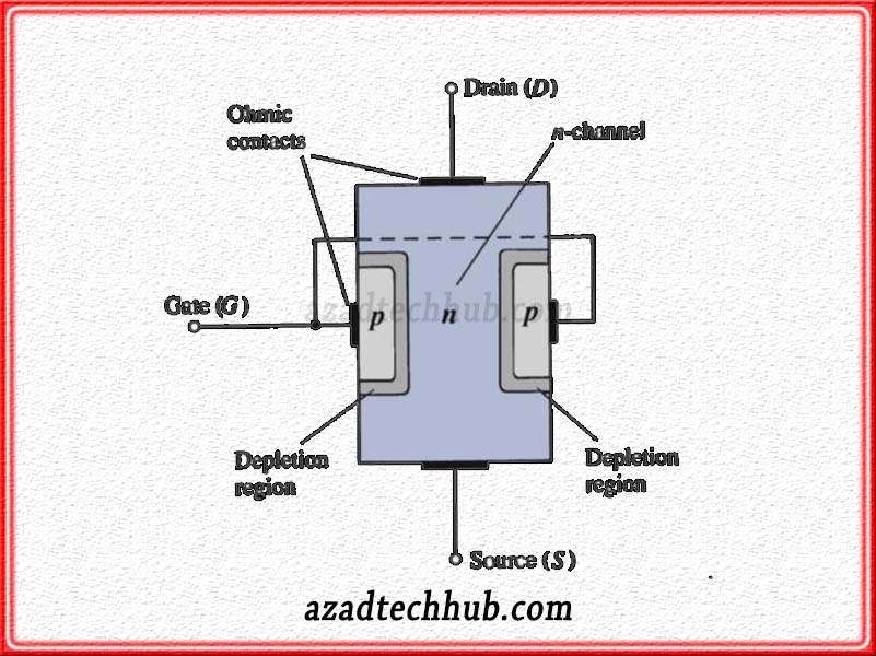
On the other hand, when we apply the reverse voltages or “-Vgs” across the source and gate, then the depletion region widens. Hence it reduces the conduction of electrons through the channel and the current decreases.
So, we are clear that when we apply voltages across the gate and source, we can control the current from the source to the drain. In other words, we can say when we apply the electric field across the gate, we can control the conduction of the junction field effect transistor (JFET). This is the reason we call this device a field effect transistor. It operates by applying the field across the gate terminal.
In the same way, the p-channel JFET works but instead of an n-type there is a p-type semiconductor material. on both ends, there are n-type semiconductors. The majority of carriers and flow of current in p-channel JFET will be because of holes instead of electrons.
Metal Oxide Semiconductor Types of Field effect Transistor (MOSFET)
A field effect transistor contains three terminals similar just like JFET but there is the main difference in gate insulation with the main channel. In MOSFET, three terminals include the same source gate and the drain terminal. But in this case, the gate is electrically insulated from the main conduction channel of MOSFET.
Therefore, we also sometimes call it the insulated gate FET which is written as “IGFET” in short form. In MOSFET, the gate current is very small either its positive gate terminal or negative one. The usage of MOSFET is the same as of JFET but in today’s modern electronics, we see MOSFET more as compared to JFET. We can classify the MOSFET into two types depletion and enhancement type of transistors. Let’s have look at enhancement type MOSFET.
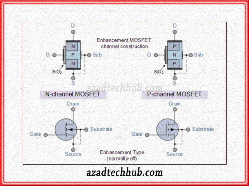
MOSFET is also available just like JFET in n-channel and p-channel and we call these MOSFET NMOS and PMOS respectively. In both types of MOSFET, the conduction of charge carriers is the as of JFET, the gate terminal produces an electric field that controls the flow of charge carriers. In the case of an n-channel, these charge carriers are electrons. But in the case of p-channel, there are holes.
Working and Operation of MOSFET
If we look at MOSFET of n-channel type, we see the source and drain connected with the n-channel through some metallic part. The gate terminal also connects through the metallic part but remains separated from the n-channel through a very narrow layer of silicon dioxide (SiO2) material. SiO2 is an insulating material and therefore no direct connection comes into place between the gate terminal and the n-channel of the MOSFET. The input impedance of the MOSFET is very high and ranges from 10^10 to 10^15 Ohms in general.
Mostly used MOSFET is of enhancement type, and in normal conditions when the gate voltage is equivalent to zero, it acts as an open switch. Now let’s assume we apply the negative potential on the gate terminal, the electrons applied on the gate will now repel the n-channel electrons. Therefore overall, in MOSFET, the number of electrons available for conduction will significantly reduce. If we further increase the negative voltage, less current will flow from the source to the drain.
What happens when we apply positive potential on the gate terminal? The gate terminal positive potential allows more electrons in the n-channel and hence more current now can flow from source to drain. Conduction channel width widens and we can say that the MOSFET conduction is increased by applying positive potential on the gate.
Follow us on LinkedIn”Electrical Insights” to get the latest updates in Electrical Engineering. You can also Follow us LinkedIn to see our latest posts.
