Common Emitter Configuration: An Important Guide
Table of Contents
Introduction
A Transistor has three basic configurations and among them, the widely used configuration is the common emitter configuration. As we know that a transistor consists of three main terminals including an emitter, a collector, and a base. These three terminals can connect to each other in three different ways and hence we can get different results or output from BJT in each configuration. From our previous article, we know that a bipolar junction transistor operates in three different modes.
In the active region, the gain of the Bipolar Junction Transistor is large and we get the collector current as a multiple of the base current. Therefore a Bipolar Junction Transistor can be used as an amplifier in the active mode of operation. While we can operate BJT as a switch in saturation and cut-off modes of operation. Read More about BJT construction and BJT modes of operation.
Configurations of BJT
As BJT has three terminals and therefore it can only connect with any other element in the circuit in three different ways. One terminal acts as the common terminal between the input and output signal in any circuit. So, in each arrangement, the output characteristics of the BJT change with the change in configuration. On the basis of the common terminal between the input and output signal, we can classify the configurations of BJT into three different types.
- The Common Collector Configuration (CC) of BJT
- The Common Base Configuration (CB) of BJT
- The Common Emitter Configuration (CE) of BJT
Common Base Configuration “CB” of BJT
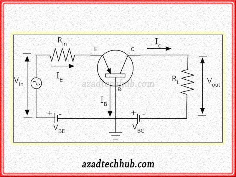
As the name depicts that the Base terminal in common base configuration is common in between the input and output signals. Input signal applies between the emitter and the Base. The output is measured between the Collector and the Base terminal. The Base in this configuration is common and is generally grounded. Let’s have a look at the below representation of the common base configuration of BJT in figure 1.
As we can see in the figure, the emitter current divides into the collector current and the base current. We can say the current on the input side is very large as compared to the output side or the collector. So, when we calculate the current gain of this circuit, we see that it comes out equivalent to unity or less than unity.
This is why the common base configuration has no current gain. But when we look at the voltage gain of this configuration, that is remarkably high due to the load resistance high values. Load resistance is very high as compared to the input resistance and therefore this configuration has some resistance gain. Which in fact increases its voltage gain. Input and output voltage signals are in phase because this configuration is non-inverting.
Common Base Configuration Circuit Diagram

Now let’s dive into formulas related to the common base configuration of BJT.
Common Base Configuration Voltage Gain
We can write the equations for Voltage gain of common base “CB” configuration as below.

As we can see in the above equation, the ratio of Ic and Ie makes the current gain which we normally denote by alpha “α”. The resistance ratio makes the resistance gain. As the RL is very high in value, therefore the voltage gain is very high in this configuration. Due to this high voltage gain, this configuration is not used more commonly. This configuration has a good response toward high frequency and we normally see this configuration in radio amplifiers or microphones where only single-stage amplification is required.
Common Collector Configuration “CC” of BJT
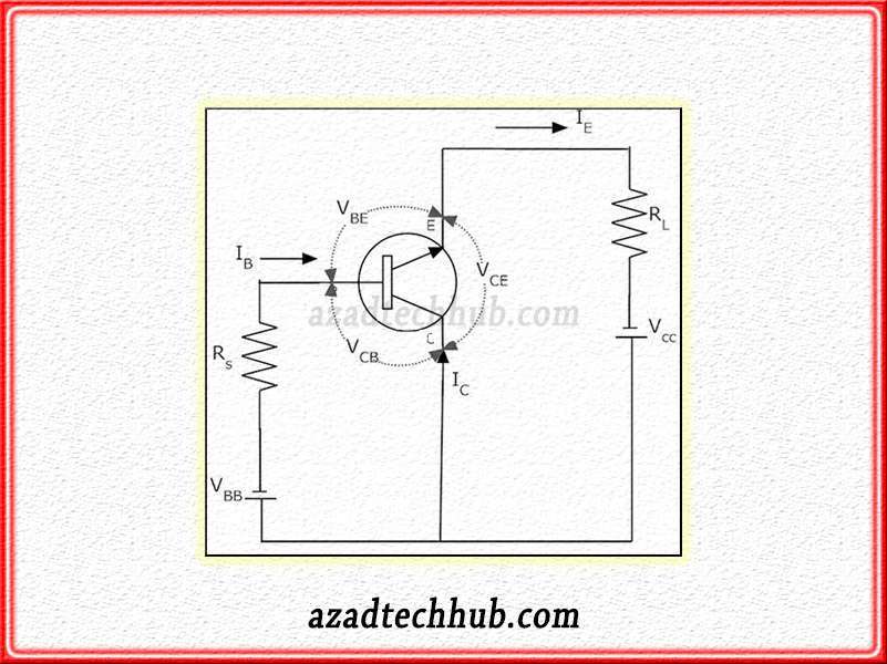
In this configuration of BJT, the collector connects with the ground through a power supply. The collector is common or grounded in between the base and the emitter terminal. We apply the input signal directly to the base terminal. The output is measured across the load resistance which is connected in series with the emitter.
We also call the common collector configuration as the voltage follower circuit or the emitter follower circuit. The input impedance of the emitter follower configuration is in the range of thousands. Therefore we use this configuration mostly in impedance-matching applications. In common collector configurations, the output impedance is very low. Let’s have a look at below figure 2 of the common collector configuration of BJT.
Common Collector Configuration Circuit Diagram

As the load resistance in series with the emitter terminal in Common Collector Configuration. So, the current through the load resistance and emitter terminal are equal. The emitter current is equivalent to the summation of the base current and the collector current. This configuration has the emitter equation as same as the common emitter configuration. We can write the current gain as below.

Common Collector Configuration Current Gain
The common collector configuration current gain can be written below.

From the current gain equation, we can say that its value will always be greater than unity. As far as the voltage gain is concerned, this configuration has a voltage gain of around unity. Therefore common collector configuration finds its applications in the voltage buffer circuits due to unity voltage gain. The other reason for buffer applications is its output voltage which is in phase with the applied input voltage as it is a non-inverting configuration.
As we see in the above figure, the load resistance is connected in series with the emitter terminal. Both currents including the base and collector flow through the load resistance. Therefore the current gain of this configuration is high and gives a good current amplification. Unlike the common emitter configuration, the common collector configuration is non-inverting.
Common Emitter Configuration (CE) of BJT
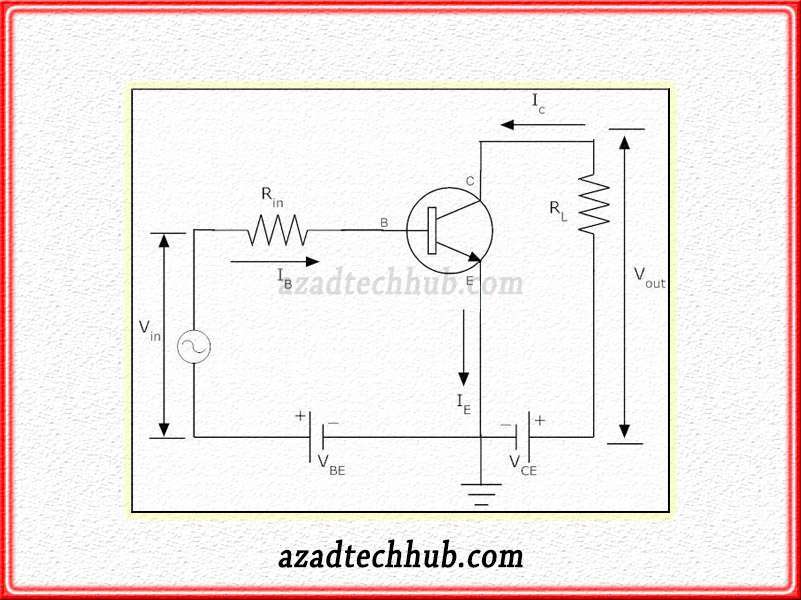
In common emitter configuration, the emitter terminal is grounded. It acts as a common terminal for the output signals and input. We apply the input in between the emitter and the base terminal while we take the output from the emitter and collector terminal. The common emitter configuration is the most used configuration for the amplifier circuits consisting of transistors among all three configurations of the BJT.
The output impedance is high due to the fact that it is from the reverse-biased PN Junction. This type of BJT configuration can also perform the function of transistor as a switch in case of PNP transistor. Where transistor is used as a switch in the circuit, base current controls the circuit switching. In this type of circuit, the base terminal is reversely biased so that it can control the circuit opening and closing. As we apply more negative voltages on the base region, there will be more flow of current. The reverse happens when we apply the positive voltages and we transistor as a switch.
The common emitter configuration produces a very high power gain and current gain. Let’s have a look at the common emitter configuration circuit diagram.
Common Emitter Configuration Circuit Diagram

The emitter current is IE which flows out of the transistor while IC and IB flow into the transistor. The current flowing inside must be equal to the outflowing current which is a combination of IC and IB. Therefore we can write the emitter current as the below equation.

As the load resistor, RL connects in series with the collector in a common emitter configuration of BJT. Therefore the collector’s current to base current ratio is high as there is a very small base current. This ratio we can call as the Beta “β”.

So, we can vary the collector current by just a small variation in the base current. In common emitter configuration, the emitter current is a summation of base and the collector current. And the ratio of collector and emitter current refers to as alpha “α”.

Further combining the relationships for alpha and beta we can write further equations for the common emitter configuration as below.

And Also


We see common emitter configuration of BJT in every other circuit. The main reason is its power gain and current gain which are the highest as compared to other schemes. The common emitter configuration has a very low voltage gain. The input signal and the output signal are not in phase. The common emitter configuration output signal is 180 degrees out of phase. Therefore we can say this configuration is an inverting circuit. The values for the Beta vary between 20 to 100. We can control the collector current with just a small change in the base current.
Also read about BJT Modes, Field Effect Transistors, and Operational Amplifiers. Want to know how transistors as a switch works? follow the link to read more about it.
Follow us on LinkedIn”Electrical Insights” to get the latest updates in Electrical Engineering. You can also Follow us LinkedIn to see our latest posts.


