The Essential Guide to CD4011 NAND Gate in Digital Circuits
Table of Contents
Introduction
The CD4011 NAND gate is one of the most commonly used gates in digital electronics because of its simplicity and versatility. The CD 4011 is a CMOS quad two-input NAND gate integrated circuit (IC) that is commonly used in digital circuits. It is a member of the CD4000 series of CMOS ICs that operate at very low power consumption and have a wide operating voltage range.
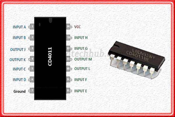
The CD4011 consists of four independent two-input NAND gates, each with its own input and output. The input signals are applied to the two input pins of the gate, and the output is obtained from the output pin. The gates are designed to operate with a power supply voltage range of 3V to 15V, making them suitable for use in a wide range of applications.
The CD4011 NAND gate has a number of advantages over other logic gates. For example, it has a very low power consumption, which makes it ideal for battery-powered devices. It also has a high noise immunity, which means that it can operate reliably even in noisy environments. Additionally, it has a wide operating temperature range, which makes it suitable for use in a variety of environments.
One of the key features of the CD4011 NAND gate is its ability to perform logical operations on binary data. When the two input pins are connected to a logic high (1), the output pin will be at a logic low (0), and vice versa. This allows the gate to perform logical operations such as AND, OR, and NOT. By combining multiple NAND gates together, more complex logic functions can be created, such as flip-flops, counters, and shift registers.
What is a NAND Gate?
A NAND gate is a digital logic gate that produces an output signal that is the opposite of the AND gate. The term NAND is a combination of the words NOT and AND. The logic symbol for a NAND gate is a triangle with a small circle on the end and two inputs.

In a NAND gate, if both inputs are high (1), the output will be low (0). In all other cases, the output will be high (1). This means that a NAND gate produces a low output only when both of its inputs are high.
The truth table for a two-input NAND gate is as follows:
| Input A | Input B | Output |
| 0 | 0 | 1 |
| 0 | 1 | 1 |
| 1 | 0 | 1 |
| 1 | 1 | 0 |
There are several types of logic gates used in digital electronics, including AND gates, OR gates, NOT gates, XOR gates, and NAND gates. Each type of gate has a specific logic function, and they can be combined to create more complex circuits.

The CD 4011 NAND gate is an essential component in many digital circuits due to its low power consumption, high noise immunity, and wide operating temperature range. It is a quad two-input NAND gate that can perform logical operations on binary data, making it a versatile and reliable digital logic gate. In this article, we provided an overview of what a NAND gate is, how it works, and its truth table. We also explained the importance of NAND gates in digital circuits and provided an overview of different types of logic gates.
CD4011 NAND Gate Features
The CD4011 NAND gate is a versatile digital logic gate that offers several features and capabilities. Here are some of its key features:
- Quad two-input NAND gate: The CD 4011 includes four independent two-input NAND gates on a single chip, providing flexibility for designing digital circuits.
- Low power consumption: The CD4011 NAND gate operates at a low power consumption, making it suitable for use in battery-powered devices.
- High noise immunity: The CD4011 NAND gate has a high noise immunity, which means that it can operate reliably in noisy environments.
- Wide operating temperature range: The CD4011 NAND gate can operate in a wide temperature range, making it suitable for use in a variety of environments.
CD4011 NAND Pins Configuration
The pin description of the CD4011 NAND gate are as follows:
- Pin 1: Input A of gate 1
- Pin 2: Input B of gate 1
- Pin 3: Output of gate 1
- Pin 4: Input A of gate 2
- Pin 5: Input B of gate 2
- Pin 6: Output of gate 2
- Pin 7: VDD (power supply)
- Pin 8: Input B of gate 3
- Pin 9: Input A of gate 3
- Pin 10: Output of gate 3
- Pin 11: Input B of gate 4
- Pin 12: Input A of gate 4
- Pin 13: Output of gate 4
- Pin 14: VSS (ground)
The CD4011 NAND gate is often compared with other types of NAND gates, such as the CD4012 and CD4013. While the CD4011 and CD4012 both have four independent NAND gates, the CD4013 is a dual D flip-flop. The CD 4011 NAND gate has a wider operating voltage range than the CD4012 and can operate at a lower voltage than the CD4013.
Ratings of CD4011 NAND Gate
The maximum ratings and recommended operating conditions for the CD 4011 NAND gate are as follows:
- Maximum Ratings:
- Supply voltage: 18V
- Input voltage: VSS-0.5V to VDD+0.5V
- Output current: 10mA
- Storage temperature range: -65°C to 150°C
- Recommended Operating Conditions:
- Supply voltage: 3V to 15V
- Input voltage: VSS-0.5V to VDD+0.5V
- Operating temperature range: -55°C to 125°C
Applications of CD4011 NAND Gate
The CD4011 NAND gate has several applications in digital circuits. Some of its common uses include:
Logic gates: The CD4011 NAND gate can be combined with other logic gates to create more complex circuits, such as flip-flops, counters, and shift registers.
Oscillators: The CD 4011 NAND gate can be used in oscillator circuits to generate square wave signals.
Inverter circuits: The CD 4011 NAND gate can be used as an inverter by connecting both inputs together.
Schmitt trigger circuits: The CD 4011 NAND gate can be used as a Schmitt trigger, which is a circuit that converts a noisy input signal into a clean output signal.
Examples of projects using the CD4011 NAND gate include digital clocks, frequency counters, and traffic light controllers. The CD4011 NAND gate’s low power consumption and high noise immunity make it ideal for use in these types of projects.
Advantages & Disadvantages
Advantages of using the CD4011 NAND gate include its versatility, low power consumption, high noise immunity, and wide operating temperature range. The CD4011 NAND gate’s quad two-input NAND gate design also makes it easy to integrate into digital circuits.
One of the disadvantages of using the CD 4011 NAND gate is its slow switching speed compared to other types of NAND gates. This can limit its use in high-speed applications.
In summary, the CD4011 NAND gate is a versatile digital logic gate that offers several features and capabilities. Its low power consumption, high noise immunity, and wide operating temperature range make it suitable for use in a variety of digital circuits. It is commonly used in projects such as digital clocks, frequency counters, and traffic light controllers. However, its slower switching speed may limit its use in high-speed applications.
Circuit Design with CD4011 NAND Gate
Designing a circuit using the CD4011 NAND gate can be a straightforward process. First, determine the desired output and identify the inputs required to produce that output. Then, use the truth table for the two-input NAND gate to determine the appropriate inputs and their corresponding states to produce the desired output. Connect the inputs and outputs to the appropriate pins on the CD 4011 NAND gate according to the pin diagram and recommended operating conditions.
Different types of circuits that can be designed using the CD4011 NAND gate include flip-flops, counters, oscillators, and more. In flip-flops, the CD 4011 NAND gate is used to store and manipulate binary data. Then in counters, it is used to count input pulses and produce an output signal based on the count. In oscillators, it is used to generate a periodic waveform with a specific frequency.
When designing a circuit using the CD4011 NAND gate, it is important to consider potential issues. Such as noise and interference. It is also important to properly choose the input and output voltages. As exceeding the maximum ratings for the CD4011 NAND gate can damage the device.
Troubleshooting and debugging a circuit design can be a time-consuming process. Some tips for debugging a circuit using the CD 4011 NAND gate include checking for incorrect wiring, incorrect component values, and checking for voltage drops or fluctuations.
Complex Circuits with CD4011 NAND Gate
The CD4011 NAND gate is commonly employ in complex digital circuits, often in conjunction with other types of logic gates such as AND gates, OR gates, and XOR gates. These circuits can perform in a variety of applications such as microcontrollers, digital signal processors, and more.
One example of a complex circuit that uses the CD4011 NAND gate is the digital clock. The CD 4011 NAND gate is used to create the flip-flops. That store and manipulate the binary data used to display the time. Other logic gates such as AND gates and OR gates are used to control the display and generate the clock signal.
Compared to other types of logic gates used in complex circuits. The CD 4011 NAND gate offers low power consumption and high noise immunity, making it a popular choice for digital circuits that require low power consumption and high noise immunity. However, its slower switching speed may limit its use in high-speed applications. Other logic gates such as AND gates and XOR gates offer faster switching speeds. But may not offer the same level of noise immunity.
Advancements in CD4011 NAND Gate Technology
The CD4011 NAND gate has been a popular choice for digital circuits for many years, but advancements in technology could lead to even more improvements in its functionality and performance. Some potential advancements in CD 4011 NAND gate technology include reducing power consumption, increasing switching speed, and improving noise immunity.
Reducing power consumption could make the CD4011 NAND gate even more useful in low-power digital circuits. Increasing switching speed could make it more versatile and useful in high-speed applications. Improving noise immunity could make it more reliable in noisy environments, such as in automotive or aerospace applications.
In addition, advancements in manufacturing technology could lead to smaller and more compact CD4011 NAND gates, which could be useful in miniaturized devices such as wearable electronics or medical implants.
CD4011 NAND Gate vs Other NAND Gates
While the CD4011 NAND gate offers many advantages such as low power consumption and high noise immunity, there are other types of NAND gates that may be better suited for certain applications.
For example, the 74HC00 is a high-speed CMOS NAND gate that offers faster switching speeds than the CD4011 NAND gate. It also offers low power consumption and high noise immunity, making it a popular choice for digital circuits that require high speed and high reliability.
Another example is the CD4012 dual 4-input NAND gate, which offers more inputs than the CD4011 NAND gate. This can be useful in circuits that require more complex logic operations or more inputs.
Ultimately, the choice of NAND gate depends on the specific requirements of the digital circuit. Factors such as power consumption, switching speed, and noise immunity must be carefully considered to determine which type of NAND gate is best suited for a particular application.
Conclusion:
In conclusion, the CD4011 NAND gate is a versatile and widely used component in digital circuits. It offers many advantages such as low power consumption and high noise immunity, making it a popular choice for a wide range of applications.
The datasheet provides engineers and designers with the information they need to design and implement circuits using the CD 4011 NAND gate. By understanding the features and capabilities of the CD4011 NAND gate, designers can create innovative and efficient digital circuits that meet the specific needs of their applications. We encourage readers to try designing their own circuits using the CD 4011 NAND gate and explore the many possibilities it offers in the world of digital electronics.
Follow us on LinkedIn”Electrical Insights” to get the latest updates in Electrical Engineering. You can also Follow us on LinkedIn and Facebook to see our latest posts on Electrical Engineering Topics.
Worth Read Posts
- What is a Variable Resistor?
- Lithium Ion Batteries
- CR2032 Battery
- Methods of Electrical Earthing
- Electrical Earthing Important Types
- Plant Factor, Plant Capacity Factor, and Load Factor
- Buck Converter Interview Questions
- DC DC Converter Interview Questions
- Transformer Electrical Interview
- Top 30 Op Amp Interview Questions
- Power Electronics Interview Questions


